Objective
This example includes several simple examples of the Configurable Custom Logic (CCL) using the SAM L21 Xplained Pro Development Board.
Materials
Hardware Tools
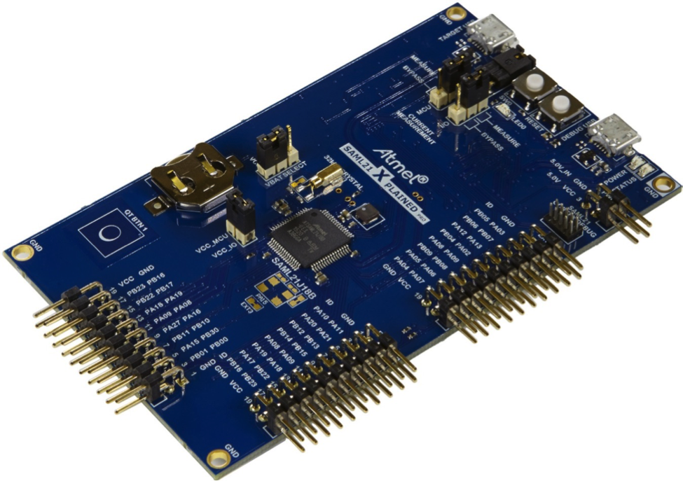
SAM L21 Xplained Pro
Software Tools
| Tool | About | Installers |
Installation
Instructions |
||
|---|---|---|---|---|---|
| Windows | Linux | Mac OSX | |||
 Atmel® Studio
Integrated Development Environment |
| | | | |
Exercise Files
| File | Download |
Installation
Instructions |
||
|---|---|---|---|---|
| Windows | Linux | Mac OSX | ||
|
Project and Source Files
|
| | | |
Additional Files
| Files |
|---|
Procedure
There are several simple projects shown in this training and all require the same initial setup. You can select the various configurations by entering the ID number of the desired configuration through the Universal Asynchronous Receiver Transmitter (UART). Additionally, (by uncommenting two lines in main) you can sequence through the configuration by pushing SW0. The Debug UART is used both for this operator entry as well as to output the ID of the present configuration. The program is structured to easily allow more demo configurations to be added. Currently, all the project configurations are in system_saml21.c; the specific function names are listed with each project description below.
Setup for all Projects
1
Task 1 - Hardware Setup
Setup of the SAM L21 Xplained Board
a
Task 1a
Jumper EXT1 Pin 3 to EXT2 pin 9 (PB05 to PB14). This is to make the PIT7 signal an input to LUT3.
b
Task 1b
Jumper EXT1 pin 10 to EXT2 pin 10 (PA02 to PB15). This is to make the button push at SW0 an input to LUT3.
c
Task 1c
Connect the board to your computer via the DEBUG USB connection.
2
Task 2 - Firmware
This is a collection of configuration routines to set up the CCL in ways that show the nuts and bolts of the many of the possible connections. All the code is in bare metal. To speed up the analysis of the various configurations, all configurations are in one program.
After reset, many of the peripherals are set up to provide inputs to the CCL. These inputs include the General Purpose Input/Output (GPIO), Timer, and Event Channel inputs. Wherever possible, the intermediate signals are brought out to pins for analysis. Once initialization is complete, only LUT3 is enabled to gate two GPIO pins to drive LED0. The signals are a ½ Hz signal from GPIO to SW0 with a Real-Time Clock (RTC) signal.
Here are some details that apply to all the configurations:
a
Task 2a
OSC16M selected to supply 8 MHz.
b
Task 2b
Since you can feed any asynchronous clock to both the CCL and individual Event System Channels, we provide a couple in case you want to experiment:
a) Set up Clock Generator 2 to use OSCULP32K and divide down to 4 kHz to experiment with supplying different asynchronous.
b) Set up Clock Generator 3 to use OSCULP32K and divide down to 64 Hz to experiment with supplying different Generic Clocks (GCLKs) (asynchronous clocks) to different peripheral blocks for SW0 debouncing purposes.
c
Task 2c
Since much of the processing is internal to the Input Capture (IC), we set up the pins to allow intermediate signals to be viewed.
d
Task 2d
SW0 input at PA2.
e
Task 2e
Jumper PA2 to a LUT input pin.
f
Task 2f
Set up TC3 as our general use timer with rollover and interrupts at 8 msec.
g
Task 2g
Set up TC0/1/2 as PWMs with 50% duty and 1.3 MHz frequency.
h
Task 2h
Set up and use the Event System to synchronize the start times of TC0/1/2.
i
Task 2i
Set up TCC0/1/2 as PWMs with 10% duty and 7.8 kHz frequency.
j
Task 2j
Set up and use the Event System to synchronize the start times of TCC0/1/2.
k
Task 2k
Set up RTC with period events at various frequencies – run these signals through event system out to GPIO to be available as LUT inputs.
l
Task 2l
Set up events system channels for PER0 and PER7.
m
Task 2m
Have events channels drive pins to:
a) Demonstrate how any LUT can drive any pin on the part.
b) Jumper PIT signal to a LUTs (by using GPIO).
The following table describes the peripherals, signals, and GPIO where signals can be viewed.

Another way to understand the setup is to look at it graphically routed through the Event System depicted below.

Some items worth noting:
- Neither Channel 2 or 4 have input events. This is because we are only triggering them by the SW command when we want to start the two groups of timers.
- Channels 0,1, and 3 are used simply to bring events out to pins.
- The Port module in the upper right works as follows:
- Any PORT event can select any Event system channel(s) as its input.
- Any Port Event can select any GPIO on the part (only one at a time, though).
- A given GPIO can be driven by up to four events, each with different actions if desired. See the spec for the priority of simultaneous incoming events.
- GPIO actions taken on an incoming event from its PORT event include:
- Pass the event through unchanged. This option has zero latency. We use this option twice - for the PER0 and the LUT3 output.
- Set pin.
- Clear pin.
- Toggle pin. We use this option once – for the PER7 output.
Project Demo 0
This project demonstrates ANDing two GPIO signals and putting the result out to two different GPIOs. Specifically, we are:
- Bringing in a 1/2 Hz square wave and output of SWO. These feed IN[0] and IN[1], respectively of LUT3.
- The truth table is set up to AND these signals.
- The ANDed result is sent to two places:
- The only GPIO eligible for the “LUT 3 OUT” signal (PB17).
- The GPIO that drives LED0 on the Xplained PRO board. The internal routing is via Event System (EVSYS) Channel 3. This step demonstrates how to extend LUT outputs to any pin on the part.
Function: void init_CCL_LUT3_to_AND_GPIOs(void)
Everything is handled with one custom function void init_CCL_LUT3_to_AND_GPIOs(void).
The function performs the following steps:
- Set up the synchronous clock to CCL
- Set up pins designated as inputs to LUT (see data sheet “Table 7-1. PORT Function Multiplexing”) in the PORT - I/O Pin Controller fields
- Disable LUT and CCL
- For two inputs of LUT, configure IO pins as input
- Disable the sequential logic
- Set the truth table to AND input from PER7 signal with SWO input with the third input to the LUT masked
- Enable the EVENT Output of LUT
- Set up the Event Channel to take in the LUT OUT signal
- Set up the synchronous clock to EVSYS
- Set up the asynchronous clock to EVSYS Channel you plan to use (each channel picks its own asynchronous clock)
- Have one of the EVSYS channels select the LUT OUT signal
- Enable one of the EVSYS channels as asynchronous
- Set up EV OUT2 signal from Event System to drive PB10
- Set GPIO connected to LED0 to select the EVOUT signal
- Have an EV OUT signal select the event channel fed by the LUT

Observation:
- Button is blinking on/off at a 1 Hz rate with button-up.
- Push button down and LED0 stops blinking and holds its state.
Project Demo 1
This project demonstrates the effect of an Edge Detector on the LUT output. It processes identical inputs with and without Edge Detection and outputs it to GPIO.
Function: void init_CCL_edge_detect_demo(void)
Everything is handled with one custom function void init_CCL_edge_detect_demo(void)
The function configures the following:
- Synchronous and asynchronous clocks for the CCL are set up as in example ID 0.
- Set up three LUTs with identical inputs. Each LUT takes in two Pulse Width Modulation (PWM) signals, one generated by a Timer Clock (TC) and the other generated by a Timer Counter for Control Applications (TCC).
- The TCs (TC0/1/2) are set up identically with their start times synchronized.
- Similarly, the three TCCs (TCC0/1/2) are set up identically (although at a lower frequency and duty cycle than the TCs) with their start times synchronized as well.
- The TCs and TCCs are NOT synchronized with each other. This is to show the effect on the output of using asynchronous inputs.
- The difference between the three LUTs is that the Truth table and the Edge Detection controls are set up as:

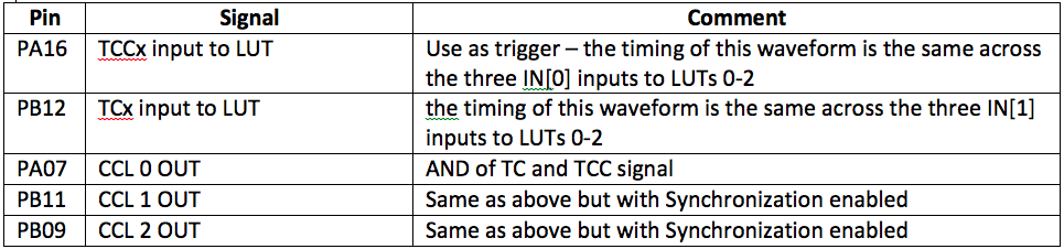
Scope Probe points:

Observations:
- Output of LUT0 represents the ANDing of two internal signals and outputting the result to one of the LUTs output pins. No Edge detection is enabled.
- Outputs of LUT1 and LUT2 are 125 ns wide pulses (due to 8 MHZ clock supplied to the CCL) at leading and trailing edges, respectively, of 380 ns wide pulses from LUT0.
Since the filter is not enabled for any of the LUT outputs, and the TC and TCC inputs to any given LUT are asynchronous to each other, we can get both a variable number of pulses and runt pulses (one is circled below on the LUT0 output).

Project Demo 2
This project demonstrates synchronizing two channels.
Function: void init_CCL_synchronize_channels_demo(void)
Everything is handled with one custom function:
void init_CCL_synchronize_channels_demo(void)
Configuration: Steps 1-4 are the same as with Project Demo 1 (same inputs to all channels) but now two of the channels are put through the synchronizer.
- Synchronous and asynchronous clocks for the CCL are set up as in example ID 0.
- Set up three LUTs with identical inputs. Each LUT takes in two PWM signals, one generated by a TC and the other generated by a TCC.
- The TCs (TC0/1/2) are set up identically with their start times synchronized.
- Similarly, the three TCCs (TCC0/1/2) are set up identically (although at a lower frequency and duty cycle than the TCs) with their start times synchronized as well.

Scope Probe points:
Observations:
- Outputs of LUT1 and LUT2 are always synchronized with each other.
- With the synchronizer/filter is enabled, the output will be delayed by two to five GCLK cycles.

Project Demo 3
This project demonstrates the effect of filtering on LUT output.
Function: void init_CCL_filter_demo (void)
Everything is handled with one custom function:
: void init_CCL_filter_demo (void))
Steps 1-4 are the same as with Project Demo 2 (same inputs to all channels) but now, rather than using edge detection, we enable different synchronizing/filtering options in each channel to show the effect on both runt pulses and throughput delay.
- Synchronous and asynchronous clocks for the CCL are set up as in example ID 0.
- Set up three LUTs with identical inputs. Each LUT takes in two PWM signals, one generated by a TC and the other generated by a TCC.
- The TCs (TC0/1/2) are set up identically with their start times synchronized.
- Similarly, the three TCCs (TCC0/1/2) are set up identically (although at a lower frequency and duty cycle than the TCs) with their start times synchronized as well.
Specifically, the Truth table and Edge Detection controls for the LUT0,1, and 2 are set up as:

Scope Probe points:

Observations:
- LUT0 (neither synchronized nor filtered) still has occasional runt pulses but no discernable throughput delay.
- LUT1 (synchronized) (nothing only 1 GCLK in width) has a delay relative to the LUT0.
- LUT2 no longer has any runt pulses is further delayed relative to LUT0.

Project Demo 4
This project demonstrates the effect of the event input by the built-in Edge Detection on SAML21. This edge detector is BEFORE the LUT.
Function: void init_CCL_event_input_demo(void)
Everything is handled with one custom function:
void init_CCL_event_input_demo(void)
- Bring PER0 event into LUT0 (internally – no GPIO needed)
- Configure truth table to put PER0 through without qualification (no gating with other signals, edge detection, synchronizing, or filtering)

Scope Probe points:

Observations:
- Outputs of LUT (blue trace at the bottom) is the pulse of a single asynchronous clock width, regardless of the width of input pulse (in this case the yellow trace, which is part of an ~1 msec wide pulse).
- Edge detector is always applied to Events coming into LUTs, even if the EDGESEL bit in control fields is set to 0.
- This edge detector is before the LUT input and is distinct from that used at the output of the LUT (the one used in DEMO ID 1). The next two scope shots are obtained by setting the truth table to take in an event as high for the first plot and low for the next plot. Note that the pulse is triggered off the leading edge regardless.


Conclusions
This series of projects will give you a better understanding of the CCL for any future projects that will benefit from code independent logic.
|
Table of Contents
|