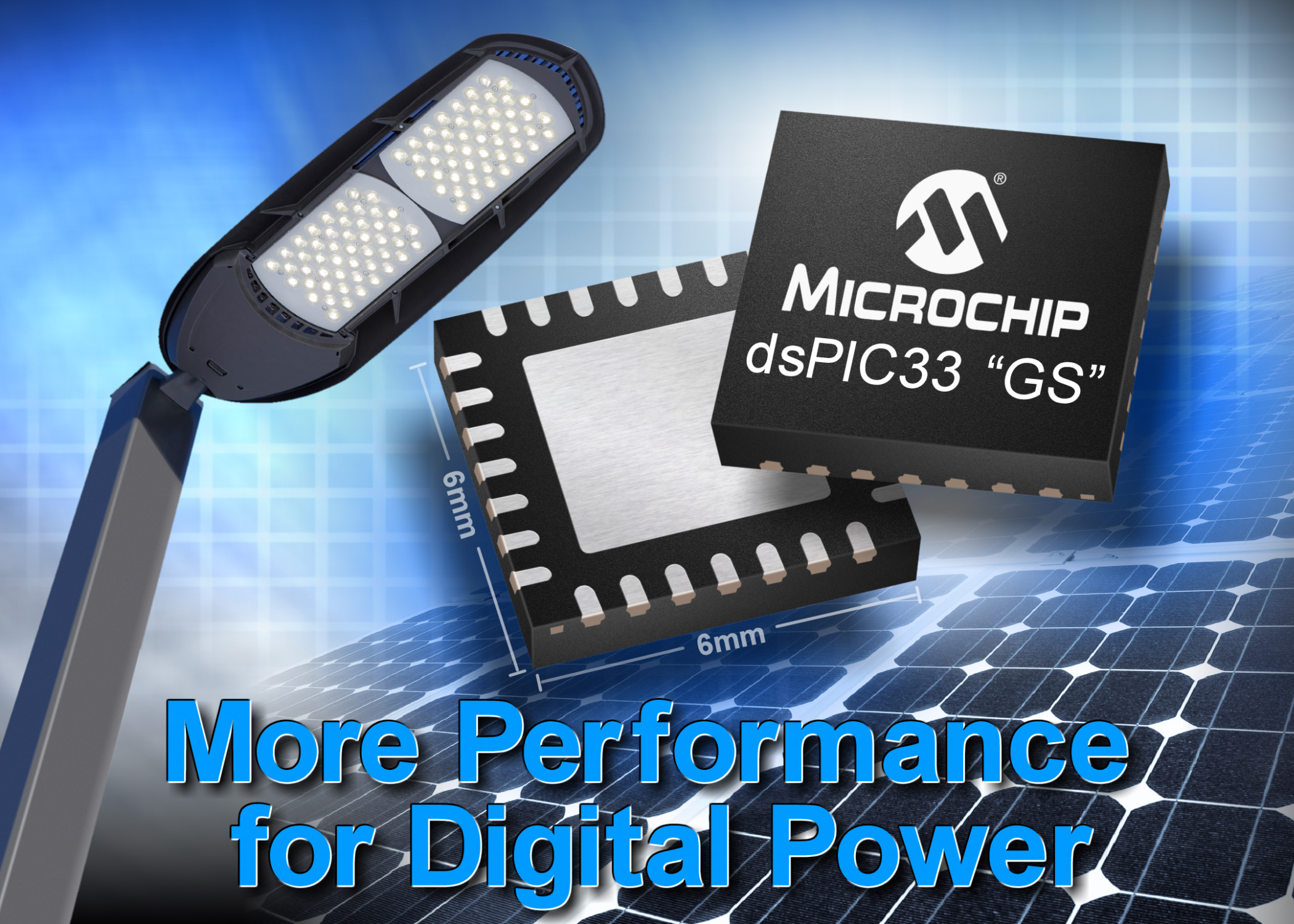
dsPIC® DSC Compartor
On-chip comparators are commonly found in microcontrollers as peripherals. There is, however, a fundamental difference between the comparators implemented in the Switch-Mode Power Supply (SMPS) device, i.e. dsPIC® DSC, and "traditional" comparators found in other microcontrollers. Generally speaking, the SMPS comparator is much faster at detecting transient conditions and measuring voltage and current in a power conversion application. In many cases, the comparators' performance often times mimics the performances of the stand-alone high-performance comparators. Because of this high-performance capability, power supply designers no longer are required to use external comparator ICs. Use of the dsPIC® DSC comparators, can reduce the overall system costs, as well as the system complexity. The figure below shows the dsPIC33 “GS” DSCs analog comparator's availability.

Comparator Features
- Up to 4 analog comparators
- 20 ns response time/ 5 mV offset voltage
- 10-bit DAC for each analog comparator
- DAC reference output
- Programmable references
Comparator Block Diagram
Below shows the high-level block diagram of the internal comparator found in the dsPIC® DSC devices. The non-inverting (positive terminal) input is connected through a multiplexer with a number of inputs pins. Each comparator can be connected to four different analog-input pins. The inverting input is internally connected to a 10-bit DAC that can be adjusted through the internal CPU bus. The CPU can write any values to the DAC register and the threshold can dynamically change in real-time. The comparator is followed by a logical block that can change the comparator output polarity. It can also be used to perform as a filter to remove glitches. The comparator can also generate a number of signals:
- Interrupt Request
- Status bit (set when the comparator output trips)
- ADC Sample-and-Convert Process
- PWM trigger
- Truncate the PWM signal (current limit)
- Truncate the PWM periods (current minimum)
- Disable the PWM outputs (Fault latch)
The comparator module can also be used to wake up the system from Sleep or Idle mode when the analog input voltage exceeds the programmed threshold voltage.

Power Conversion Applications Using Comparator
The two most common comparator features used in power conversion applications are:
- Control loop: The comparators are used to detect the peak current value and consequently shut down the PWM output. This is similar to what the comparator does in the analog domain in peak current mode control.
- Monitor over-current and/or over-voltage events: To immediately shut down the PWM outputs to prevent the unit from being damaged.
Both features require the comaparator to have at least two characteristics:
- Speed: The comparator needs to respond quickly when an over-current event occurs. Speed is measured by the propagation delay, which is the time required for the comparator to change state when the input value changes crossing the predefined comparator threshold.
- Accuracy: The input threshold needs to be precisely defined and the comparator output will change as soon as the input signal crosses this threshold, i.e. the offset defines how precisely the signal crosses the threshold.
Note:
Propagation delay is measured from the analog input to the PWM output pin.
The SMPS dsPIC® DSC on-chip comparators characteristics:
- Offset:
- Typical: +/- 5 mV
- Max: +/- 15 mV
- Propagation delay:
- Typical: 20 ns
- Max: 30 ns
Indeterminate Output:
- The comparator has a limitation for the input Common-Mode Range (CMR) of: Analog VDD – 1.5 volts, typical. This means that both inputs should not exceed this range. As long as one of the inputs is within the Common-Mode Range, the comparator output will be correct. However, any input exceeding the CMR limitation will cause the comparator input to be saturated. If both inputs exceed the CMR, the comparator output will be indeterminate.
- The DAC has a limitation for the maximum reference voltage input of: Analog VDD – 1.6 volts. An external reference voltage input should not exceed this value or the reference DAC output will become indeterminate.
Leading-Edge Blanking
Leading-Edge Blanking (LEB) a useful feature for filtering out the switching noise that is usually coupled into the input signals, e.g. supply transient current. The noise could also be generated by the PWM switching and the glitches may be too high that the comparator will erroneously trip (false trigger) due to these transient spikes. To avoid this, the LEB essentially blanks the input signal for a programmable time duration. This time interval can go from 0 to 1,023 nanoseconds, with a step size of 8 nanoseconds.

Note:
The comparator is configured during the initialization routines which are called from the main program at the start of the execution. It is important that none of the peripherals are enabled before the entire peripheral configuration is completed.
dsPIC® DSC Comparator in Single-Phase Buck Converter Application
The Single-Phase Buck Converter uses the peak current mode control. The control scheme is shown below. The control loop is implemented by utilizing the dsPIC® DSC analog comparator module and varying the programmable threshold in software. The Buck MOSFET current is sensed using a current transformer and fed directly to the analog comparator input.

The measured output voltage is compared with the reference to produce the voltage error. The voltage error compensator is then executed and a current reference value is obtained. The analog comparators on the dsPIC33FJ16GS504 have built-in programmable Digital-to-Analog Converters (DACs) that determine the comparator's threshold. The calculated current reference is used to set a new threshold for the analog comparator. The output voltage is measured using the analog input. The analog comparator input is connected to the output of the current transformer.
When the inductor current signal exceeds the programmed threshold, the comparator terminates the PWM pulse. This termination of the PWM pulse effectively modifies the ON time for the PWM signal to control the output voltage.
Note:
- The comparator resource names vary from device to device. Please refer to the specific dsPIC® DSC device data sheet for details.
- The following registers control the comparator module:
- CMPCONx: Comparator Control x Register
- CMPDACx: Comparator DAC Control x Register